- 您现在的位置:买卖IC网 > Sheet目录234 > MAX3205EATE+ (Maxim Integrated Products)IC ESD PROT DIFF 16-TQFN
�� �
�
�Dual,� Quad,� and� Hex� High-Speed�
�Differential� ESD-Protection� ICs�
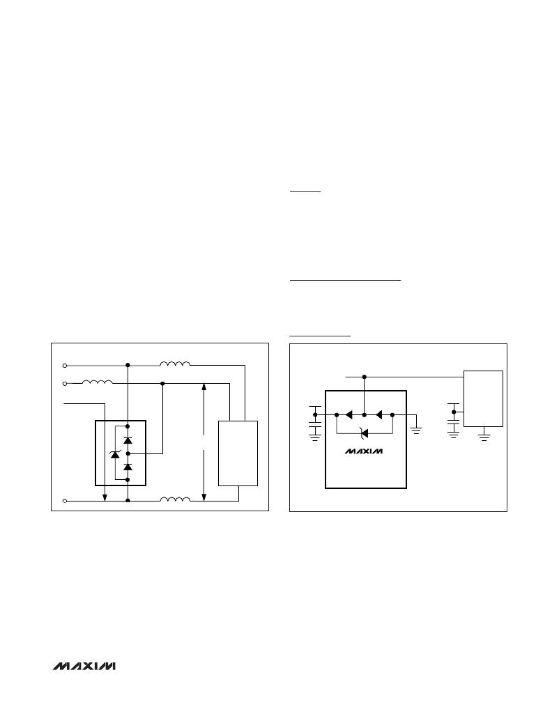
�Layout� Recommendations�
�Proper� circuit-board� layout� is� critical� to� suppress� ESD-�
�induced� line� transients� (See� Figure� 6).� The� MAX3205E/�
�MAX3207E/MAX3208E� clamp� to� 100V;� however,� with�
�improper� layout,� the� voltage� spike� at� the� device� can� be�
�much� higher.� A� lead� inductance� of� 10nH� with� a� 45A�
�current� spike� results� in� an� additional� 450V� spike� on� the�
�protected� line.� It� is� essential� that� the� layout� of� the� PC�
�board� follows� these� guidelines:�
�1)� Minimize� trace� length� between� the� connector� or�
�input� terminal,� I/O_,� and� the� protected� signal� line.�
�2)� Use� separate� planes� for� power� and� ground� to� reduce�
�parasitic� inductance� and� to� reduce� the� impedance� to�
�the� power� rails� for� shunted� ESD� current.�
�3)� Ensure� short� low-inductance� ESD� transient� return�
�paths� to� GND� and� V� CC� .�
�4)� Minimize� conductive� power� and� ground� loops.�
�5)� Do� not� place� critical� signals� near� the� edge� of� the� PC�
�6)� Bypass� V� CC� to� GND� with� a� low-ESR� ceramic� capaci-�
�tor� as� close� to� V� CC� as� possible.�
�7)� Bypass� the� supply� of� the� protected� device� to� GND�
�with� a� low-ESR� ceramic� capacitor� as� close� to� the�
�supply� pin� as� possible.�
�WLP� Applications� Information�
�For� the� latest� application� details� on� WLP� construction,�
�dimensions,� tape� carrier� information,� printed� circuit�
�board� techniques,� bump-pad� layout,� and� recommend-�
�ed� reflow� temperature� profile,� as� well� as� the� latest� infor-�
�mation� on� reliability� testing� results,� refer� to� Application�
�Note� 1891:� Wafer-Level� Packaging� (WLP)� and� Its�
�Applications.�
�Chip� Information�
�PROCESS:� BiCMOS�
�board.�
�V� CC�
�L2�
�Typical� Operating� Circuit�
�L1�
�I/0� LINE�
�I/0�
�PROTECTED� LINE�
�V� CC�
�I/0_�
�V� CC�
�PROTECTED�
�CIRCUIT�
�NEGATIVE� ESD-�
�CURRENT�
�PULSE�
�PATH� TO�
�0.1� μ� F�
�0.1� μ� F�
�GROUND�
�D1�
�I/O_�
�V� C�
�PROTECTED�
�D2�
�CIRCUIT�
�MAX3205E�
�MAX3207E�
�MAX3208E�
�GND�
�Figure� 6.� Layout� Considerations�
�L3�
�_______________________________________________________________________________________�
�7�
�发布紧急采购,3分钟左右您将得到回复。
相关PDF资料
MAX5490GA01000+T
RES NET 50K OHM 2 RES SOT23-8
MAX5491NA01500+T
RES NET MULT OHM 2 RES SOT-23
MAX5492LB10000+T
RES NET MULT OHM 2 RES SOT-23
MB2181SS2G13-CC
SWITCH PUSH 4PDT 0.4VA 28V
MB2185SB1W01-6C-A
SWITCH PUSHBUTTON 4PDT 6A 125V
MB2411JA01-G-1A
SWITCH PUSHBUTTON SPDT 3A 125V
MB2461A2W30-FA
SWITCH PUSHBUTTON DPDT 3A 125V
MB2461E1G03-HA
SWITCH PUSH DPDT 0.4VA 28V
相关代理商/技术参数
MAX3205EATE+T
功能描述:TVS二极管阵列 6Ch Differential ESD Protection IC RoHS:否 制造商:Littelfuse 极性: 通道:4 Channels 击穿电压: 钳位电压:11.5 V 工作电压:2.5 V 峰值浪涌电流:20 A 安装风格:SMD/SMT 端接类型:SMD/SMT 系列: 最小工作温度:- 40 C 最大工作温度:+ 85 C
MAX3205EATE-T
功能描述:TVS二极管阵列 RoHS:否 制造商:Littelfuse 极性: 通道:4 Channels 击穿电压: 钳位电压:11.5 V 工作电压:2.5 V 峰值浪涌电流:20 A 安装风格:SMD/SMT 端接类型:SMD/SMT 系列: 最小工作温度:- 40 C 最大工作温度:+ 85 C
MAX3205EAWL+T
功能描述:TVS二极管阵列 Dual Quad and Hex High-Speed Differential ESD-Protection ICs RoHS:否 制造商:Littelfuse 极性: 通道:4 Channels 击穿电压: 钳位电压:11.5 V 工作电压:2.5 V 峰值浪涌电流:20 A 安装风格:SMD/SMT 端接类型:SMD/SMT 系列: 最小工作温度:- 40 C 最大工作温度:+ 85 C
MAX3205EETE+
功能描述:TVS二极管阵列 6Ch Differential ESD Protection IC RoHS:否 制造商:Littelfuse 极性: 通道:4 Channels 击穿电压: 钳位电压:11.5 V 工作电压:2.5 V 峰值浪涌电流:20 A 安装风格:SMD/SMT 端接类型:SMD/SMT 系列: 最小工作温度:- 40 C 最大工作温度:+ 85 C
MAX3205EETE+T
功能描述:TVS二极管阵列 6Ch Differential ESD Protection IC RoHS:否 制造商:Littelfuse 极性: 通道:4 Channels 击穿电压: 钳位电压:11.5 V 工作电压:2.5 V 峰值浪涌电流:20 A 安装风格:SMD/SMT 端接类型:SMD/SMT 系列: 最小工作温度:- 40 C 最大工作温度:+ 85 C
MAX3206EEBL
制造商:Maxim Integrated Products 功能描述:LOW-CAPACITANCE 2/6-CHANNEL +/-15 - Rail/Tube
MAX3206EEBL+T
功能描述:TVS二极管阵列 RoHS:否 制造商:Littelfuse 极性: 通道:4 Channels 击穿电压: 钳位电压:11.5 V 工作电压:2.5 V 峰值浪涌电流:20 A 安装风格:SMD/SMT 端接类型:SMD/SMT 系列: 最小工作温度:- 40 C 最大工作温度:+ 85 C
MAX3206EEBL-T
功能描述:TVS二极管阵列 RoHS:否 制造商:Littelfuse 极性: 通道:4 Channels 击穿电压: 钳位电压:11.5 V 工作电压:2.5 V 峰值浪涌电流:20 A 安装风格:SMD/SMT 端接类型:SMD/SMT 系列: 最小工作温度:- 40 C 最大工作温度:+ 85 C